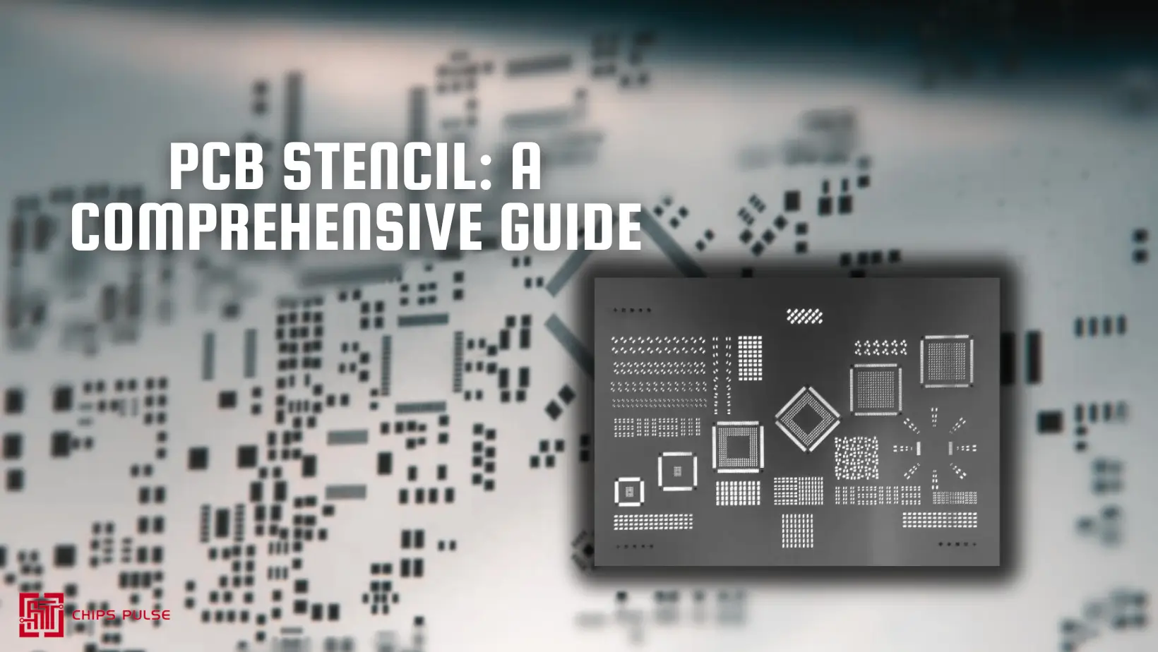
A Printed Circuit Board (PCB) Stencil serves as a vital tool in the surface mount technology (SMT) assembly process, streamlining the application of solder paste and ensuring precise component placement.
A PCB Stencil is a flat sheet of stainless steel, featuring precisely laser-cut apertures aligned with the corresponding SMT pads on a PCB. These apertures dictate where solder paste is to be deposited during the assembly process.
Facilitating Solder Paste Deposition: During SMT assembly, the PCB stencil is placed over the bare PCB board, providing a guide for the application of solder paste. This process ensures that the deposit of solder paste is accurately confined to specified locations, optimizing the alignment and connectivity of surface mount components.
Ensuring Optimal Solder Joint Quality: By accurately depositing the right amount of solder paste on the SMT pads, the PCB stencil contributes to the creation of high-quality solder joints, ensuring robust electrical connections and mechanical durability. This is crucial for the reliability and performance of electronic devices.
Enhancing Efficiency and Accuracy:The use of a PCB stencil not only expedites the PCB assembly process by simplifying the application of solder paste, but also enhances precision. The result is improved efficiency and reduced margin of error, leading to higher yields and lower rework rates in manufacturing processes.
Once the stencil is fabricated, it is carefully aligned and placed on the top of the PCB using fiducial marks, which act as positioning points to achieve perfect alignment. With the stencil in place, solder paste is applied onto the PCB using a metal squeegee blade. This results in the controlled deposition of solder paste onto the board at the precise locations where surface mount components are intended to be placed.

When developing or ordering a PCB stencil, several important points should be considered to ensure the optimal performance of the stencil in the solder paste application process. One critical factor to keep in mind is the thickness of the stainless steel sheet used for the stencil. The accurate thickness of the stencil sheet is essential as it directly impacts the release of the desired amount of solder paste through the stencil's openings.
The relationship between the thickness of the sheet and the aperture size is crucial, as these factors collectively influence the amount of solder paste that will be deposited on the board during the assembly process. If the stencil sheet is too thick, it can result in excessive solder deposition, potentially leading to solder bridging between components on the board. On the other hand, if the stencil sheet is too thin, it may lead to insufficient solder deposition, which can result in weak solder joints, compromising the functionality and reliability of the final PCB board.
Achieving the right balance between the thickness of the stencil sheet and the aperture size is crucial in ensuring that the solder paste is uniformly and accurately deposited onto the board, thus contributing to the overall quality and reliability of the assembled PCB.
To avoid these issues, it is important to work closely with experienced PCB stencil manufacturers or suppliers who can provide guidance on selecting the appropriate stencil sheet thickness and aperture size based on the specific requirements of the PCB design and assembly process. Furthermore, the use of advanced manufacturing techniques and materials can also help in achieving precise and consistent solder paste deposition, ultimately contributing to the production of high-quality PCBs